TRAPATT Diodes
Introduction :
The abbreviation TRAPATT stands for trapped plasma avalanche triggered transit mode.
It is a high efficiency microwave generator capable of operating from several hundred megahertz to several gigahertz.
Structure:

High peak power diodes are typically silicon n+-p-p+ or p+-n-n+ structures with the n type depletion region width varying from 2.5 to 12.5 µm.
The doping of depletion region is generally such that the diodes are well punched through at breakdown.
The device P+ region is kept as thin as possible at 2.5 to 7.5 µm.
The Trapatt diodes diameter ranges from as small as 50 µm for µw operation to 750 µm at lower frequency for high peak power device.
Principle of operation :

A high field avalanche zone propagates through the diode and fills the depletion layer with a dense plasma of electron & holes that become trapped in low-field region behind the zone.
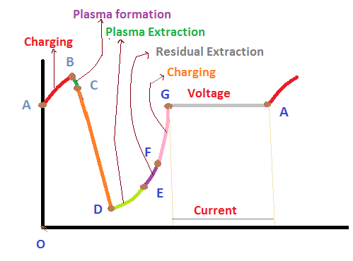
A typical voltage waveform for the TRAPATT mode of an avalanche p+-n-n+ diode operating with an assumed square wave current drive shown in figure .
A Point A the electric field is uniform throughout the sample and its magnitude is large but les than the value required for avalanche breakdown.
The current density expressed by J=6s ![]()
AT the instant of time at point A, the diode current is turned on.
Since the charge carriers present are those caused by thermal generation, the diode initially charge up like a linear capacitor, driving the magnitude of the electric field above the breakdown voltage.
When sufficient number of carrier is generated, the particle current exceeds the external current and the electric field is depressed throughout the depletion region, causing the voltage to decrease. This portion of the cycle is known by the curve from point B to point C.
During this time interval the electric field is sufficiently large for the avalanche to continue and a dense plasma of electrons and holes is created. The voltage decrease to D.
The holes produced in the avalanche rapidly reach the p+ contact taking no part in process but the electrons are released into N region where they do not combine with either doner or holes.
The electron drift at their maximum velocity across the N region and current continuous to flow in the external circuit which they are in transit.
When this current pulse actually arrives at the cathode terminal, the ac voltage is at its negative peak and the second delay of 90. (90 degree) has taken place. This time depends upon the velocity and the thickness of the highly doped N+ layer.
A large time is required to remove the plasma because total plasma charge is large compared to the charge per unit time in the external current.
At point E plasma is removed.
As the residual charge is removed, the voltage increases from point E to point F . At point F all the charge generated internally has been removed.
From point F to G the diode charged up again like a fixed capacitor.
At point G the diode current goes 0 for half period and the voltage remains constant VA until the current comes back on and the cycle repeats.


