


- The charge storage problem of P-N junction can be minimize or limited in schottky diodes.
- The potential barrier is set with a contact between a metal & semiconductor.
- The rectifying action is depends on majority carrier only.
- As the result there are is o excess minority carrier to recombination hence low level of reverse recovery time.
- These diodes are used as rectifier at a single frequency exceeding 300 MHz to 20 GHz.
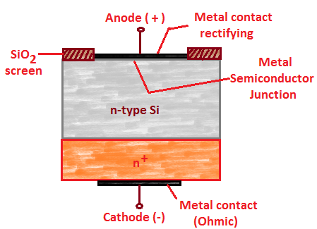
- A schottky diode is shown in figure.
- It is a metal semiconductor junction diode without depletion layer.
- On one side of junction a metal like gold, silicon, platinum is used and other side N type doped semiconductor is used.
- For protection purpose metal layer is surrounded by gold or silver layer.
- The metal film forms the positive electrode and semiconductor is the cathode.
- Operation is due to the fact that the electrons in different material have different potential energy.
- N type semiconductors have higher potential energy as compare to electrons of metals.
- When these two are brought together in contact, there a flow of electron in both direction across the metal-semiconductor interface when contact is first made.
- A voltage is applied to the schottky diode such that the metal is positive with respect to semiconductor.
- The voltage will oppose the built in potential and makes it easier to current flow.
- Schottky diode turns on and off faster than ordinary P-N junction diode the basic reason behind this is that schottky diodes are based on majority carrier.
- As there is no minority carrier there is no worry about depletion layer.
- It has much less voltage overshoot.
Schottky Diode
Introduction :


Construction:
Working:
Advantages :