IMPATT Diode (Transit-time device)
Impatt Diode is a Transit-Time device. A Transit-time device is high frequency device that operates at or above micowave frequencies.
The two important term of Impatt Diode are below -
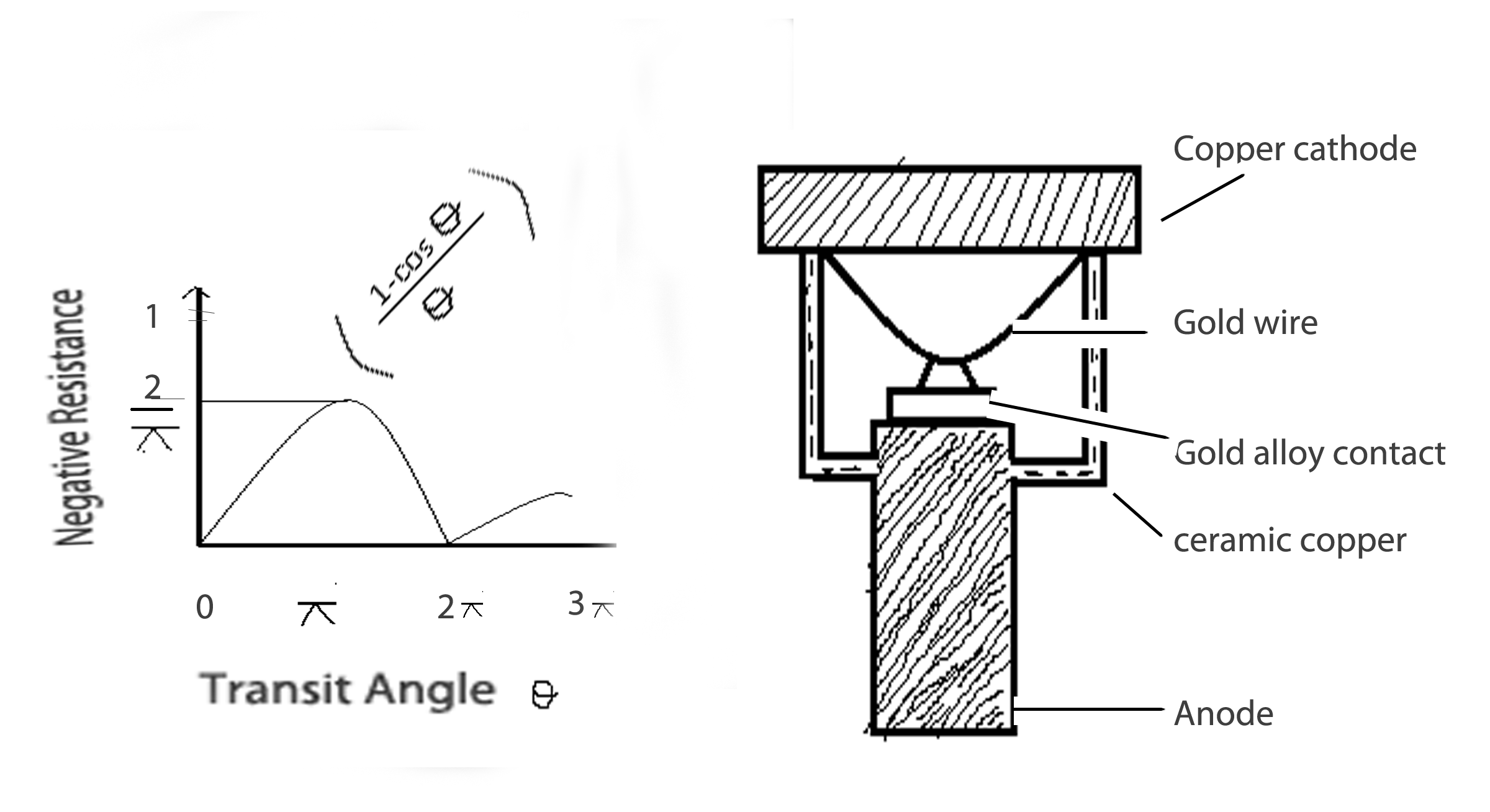
Negative Resistance : Property of device which causes the current through it to be 180 °(180 degree) out of phase with the voltage across it. Impatt diode exhibits this kind of negative resistance.
Impatt Ionization: If a free electron with suficient kinetic energy strikes a silicon atom,it can break a covalent band and lebrated from the bond .If this kinetic energy is gained from an applied electric field, the liberation of the electron from the bond is term as Impatt ionization.
Manny structure can be possible such as P+ N I N+ or P+ P N N+ as shown in figure
![]()
![]()
Construction:
IMPATT diode are made of silicon as it is cheaper and easier to fabricate using epitaxial groth.
below figure is showing a typical Impatt diode.The gold alloy contact is used as it has low ohmic and thermal resistance.

![]()
![]()
Principle of Operation : In Impatt diode extremely high voltage gradient is applied(400kv/cm)which a normal which a normal pn junction can't withstand.
Such a high potential graidient,back-biasing the diode cause a flow of minority carrier across the junction.
The ac current is approxi 180 degree out of phase with the applied voltage this gives rise to negative conduction and oscillation is resonant circuit.
Working: Figure shows a diagram of Impatt diode along with variation of average electric field
With a high bais threshold DC voltage ,as the applied ac voltage goes positive electron hole velocity become so high that these carriers form additional holes and electron by knocking them out of the crystal structure by impatt ionization.
The original DC field is just at the threshol of the allowing this situation but this threshold voltage is exceede only during the positive half cycle of A.C voltage .it is a cumulative process and takes time. A 90 degree phase difference or a delay has taken place.
The holes produced in the avlanche rapidley reach the p+ contact taking no part in the process but the electrons are released into n region where they do not combine which either donar or holes.
The electron drift at their maximam velocity across the n region and current contineous to flow in the external circuit which they are in transit.
When this current pulse actully arrives at the cathode terminal,the A.C voltage is at its negative peak and the second delay of 90 degree has taken place.This time depends upon the velocity and the thickness of the highly doped n+ layer.


