


Block Diagram of OP-AMP
The OP-Amp is basically a differential amplifier i.e. it will amplify the voltage which is differentially present between its input terminals.
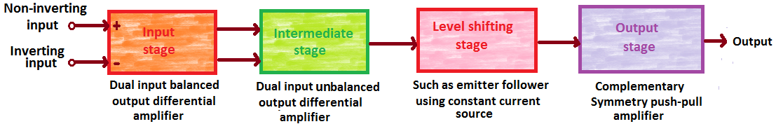
Input stage :
The input stage is a dual-input, balanced output differential amplifier. The two input are inverting and non-inverting input terminals. This stage provides most of the voltage gain of the OP-AMP and decides the input resistance value Ri.
Intermediate stage :
This is usually another differential amplifier. It is driven by the output of the input stage. This stage is a dual-input unbalanced output (single ended output) differential amplifier.
Level shifting stage :
Due to the direct coupling between the first two stages, the input of level of shifting stage is an amplified signal with some non-zero dc level. Level shifting stage is used to bring this dc level to zero volts with respect to ground.
Output Stage :
This stage is normally a complementary output stage. It increases the magnitude of the voltage and raises the current supplying capability of OP-AMP.it also provides a low output resistance.